With the development of integrated circuits to high density, miniaturization and high performance, 3D packaging technology has become an important direction in the field of semiconductor packaging. Compared with traditional 2D packaging, 3D packaging greatly improves the integration and computing efficiency of devices through vertical stacking of chips and their interconnection structures.
However, the thermal management issues, dimensional stability requirements, and package reliability challenges also place higher performance requirements on the packaging materials. Molybdenum-copper alloy (Mo-Cu) is regarded as an ideal heat sink and support material for packaging due to its excellent thermal conductivity, low coefficient of thermal expansion, and good dimensional stability. However, in the process of practical application, molybdenum and copper still face many technical challenges, and in-depth research and technological breakthroughs are urgently needed.
First of all, the problem of interfacial bonding is one of the main obstacles that limit the widespread application of molybdenum copper. Due to the large difference in the physical properties of molybdenum and copper, microscopic pores or poor metallurgical bond interfaces are easy to form in the process of sintering or liquid phase copper penetration. Especially in the multi-chip stacked structure, the materials must have excellent interfacial thermal conductivity and structural reliability, while the matching between Mo-Cu alloy and organic packaging substrate and chip metal interconnection is poor, which is prone to thermal fatigue or delamination problems during thermal cycling.
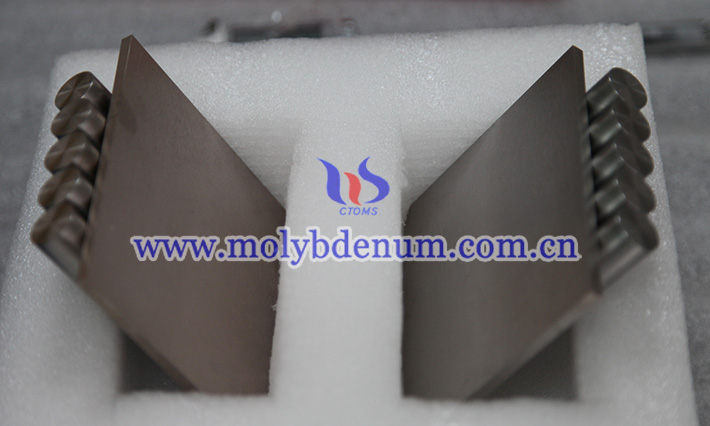
Secondly, it is difficult to control dimensional accuracy. 3D packaging requires extremely high dimensional accuracy of the packaging components, especially the stacking spacing between the chips is only a few tens of microns, and any dimensional deviation may cause package failure. Due to the preparation of Mo-Cu alloy by powder metallurgy and liquid phase permeation method, the sintering shrinkage of the material and the uneven copper seepage path may lead to dimensional instability, which further affects the subsequent processing and assembly accuracy.
Third, miniaturization technology is limited. As 3D packaging moves toward smaller sizes, Mo-Cu alloy parts also need to be ultra-thin and microstructured. Due to the high hardness, brittleness and processing difficulty of molybdenum, it is difficult for traditional machining methods to meet the needs of miniaturization and complex structure. Although advanced manufacturing technologies such as laser processing and micro-milling can be partially replaced, they still need to be improved in terms of efficiency, accuracy and material loss.
In addition, thermal stress management during the encapsulation process is complex. The heat sources between the chips are dense, the packaging structure is complex, and the temperature gradient is obvious, which is easy to generate internal thermal stress. Although Mo-Cu alloy has a low coefficient of thermal expansion and excellent thermal conductivity, it may still cause cracking, deformation or interfacial detachment due to thermal stress concentration in high-temperature welding, reflow soldering and long-term thermal cycling.
Finally, the issue of cost and process compatibility should not be overlooked. The preparation cost of molybdenum copper alloy is high, especially the high purity molybdenum powder is expensive and difficult to process, resulting in an increase in the overall packaging cost. At the same time, molybdenum-copper alloys have compatibility problems in some advanced packaging processes (such as TSV fabrication and electroplating contact), which requires adjustments or additional steps to the existing process, which affects the process efficiency.

